TUTORIAL - PART 4
15) How do the materials and designs of the on-chip contacts and interconnections affect the temperature capabilities of devices?
On-chip metallizations can be divided into two broad areas: (1) contacts to the semiconductor material or metallizations on gate insulators, (2) interconnections, including vias, between devices or to bond pads. The first generally presents the greatest problem, particularly contacts to semiconductors because of the interfaces between different materials, and thus the greater possibility for interactions or barriers to charge transfer. Primarily for high temperatures, the contacts have a major effect on temperature capability and often determine a device's practical upper temperature limit. The area of metallizations is expected to remain a bottleneck for practical application of high-temperature semiconductor devices.
With changing temperature, there will be some change in the resistivity of on-chip metallizations. At cryogenic temperatures the decrease in resistance of interconnecting metallization (Au or Al for example) can be dramatic, and has been suggested as a means to improve the performance of complex ICs.
Low temperature
As temperature is lowered, materials become very stable and interactions between materials at interfaces essentially cease because of the lack of thermal energy needed for atomic or molecular motion. Thus the contacts and interconnections (metallizations) on device die do not generally present a reliability problem at low temperatures. On the other hand, contacts to semiconductors can present a barrier to current at low temperatures under certain circumstance.
Some time ago investigators at IBM reported problems with metal films used for low-temperature (approximately 4 K) Josephson junctions. Temperature cycling resulted in film deformation thought to be responsible for junction failure. However, these films were of soft Pb alloys; subsequent use of harder materials eliminated the problem. This is the only instance of reliability difficulties with device metallizations for low temperatures that we are aware of.
High temperature
At high temperature we find the opposite. Materials generally become less stable and interactions between materials become more likely as temperature increases. Thus interdiffusion, electromigration, restructuring (voids or hillocks), oxidation or corrosion can take place rapidly. These can be further intensified by temperature cycling.
For example, GaAs devices can operate to approximately 500°C, but specialized metallization systems are necessary in order for a GaAs device to be used for even a minimum practical time (~10–100 hours) at this temperature. Likewise, the practical temperature limit for SiC devices is determined by the on-chip contacts. The devices themselves have been shown to operate to over 600°C, but SiC transistors offered commercially have so far been rated to only 350°C because of the contacts and packaging. As noted before in other contexts, the required robustness of the contact depends on the required lifetime.
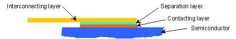
A simplified contact system for a semiconductor.
Remedies include changing to a different materials system or using more conservative designs. Contact metallizations for high-temperature can be quite complicated, since—nearly always—different materials must be used for contacting the semiconductor and for interconnecting, plus intermediate layers because of incompatibilities between the other two layers (see the figure above). For example, a Ni/Ge/Au/Ni/W5Si3/Au system was used for ohmic contacts on GaAs to attain 600 hours lifetime at 400°C [1]. What works for one semiconductor material may not work for others. Compound semiconductors (GaAs, AlGaAs, GaP, InP, GaN, SiC, ...) are more difficult than elemental semiconductors (Si or C) because of the greater number of elements and possible interactions.
[1] K. Fricke, H. L. Hartnagel, G. Schweeger and J. Wűrfl, "New technology developments for III-V semiconductor devices operating above 300°C," Fifteenth State-of-the-Art Program on Compound Semiconductors (SOTAPOCS XV), Phoenix, Arizona, 13-18 Oct. 1991, Electrochemical Society Proceedings, vol. 92-19, 1992, pp. 1-6.
The preceding has been adapted from the Extreme-Temperature Electronics Newsletter Issue #4 (22 June 2002). Please keep in mind that the above material is only a general overview; the coverage is abbreviated and many points are only touched on. Further information may be obtained from the included Internet link and from the items listed separately.
Return to top of page
¦ Part 1
¦ Part 2
¦ Part 3
Home
Most recent update: 14 January 2003
Copyright © 2002, 2003 by Randall K. Kirschman. All rights reserved.
